599,99 zł
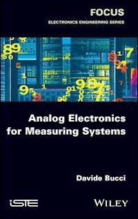
Many instrumentation engineers and scientists often deal with analog electronic issues when approaching delicate measurements. Even if off-the-shelf measuring solutions exist, comprehension of the analog behavior of the measuring system is often a necessity. This book provides a concise introduction to the main elements of a low frequency analog acquisition chain. It aims to be sufficiently general to provide an introduction, yet specific enough to guide the reader through some classical problems that may be encountered in the subject. Topics include sensors, conditioning circuits, differential and instrumentation amplifiers, active filters (mainly for anti-aliasing purposes) and analog to digital converters. A chapter is devoted to an introduction to noise and electronic compatibility. This work is intended for people with a general background in electronics and signal processing, who are looking for an introduction to classical electronic solutions employed in measuring instruments involving low frequency analog signal processing.
Ebooka przeczytasz w aplikacjach Legimi na:
Liczba stron: 192
Cover
Title
Copyright
Introduction
I.1. Purpose
I.2. Prerequisites
I.3. Scope of the book
I.4. Conventions for schematics and voltages
I.5. Acknowledgments
1 Fundamentals of Sensing and Signal Conditioning
1.1. Introduction
1.2. Voltage generating sensors
1.3. Current generating sensors
1.4. Charge generating sensors
1.5. Resistive sensors
1.6. Reactive sensors
1.7. Conclusion
2 Amplification and Amplifiers
2.1. Introduction
2.2. Introduction to operational amplifiers
2.3. Limitations of real operational amplifiers
2.4. Instrumentation amplifiers
2.5. Isolation amplifiers
2.6. Conclusion
3 Elements of Active Filter Synthesis
3.1. Introduction
3.2. Low-pass filter approximation
3.3. Active filter synthesis by means of standard cells
3.4. Frequency transform techniques
3.5. Conclusion
4 Analog to Digital Converters
4.1. Digital to analog converters and analog to digital converters: an introduction
4.2. Notations and digital circuits
4.3. Sample and hold circuits
4.4. Converter structures
4.5. No silver bullet: choosing the best trade-off
4.6. Conclusion
5 Introduction to Noise Analysis in Low Frequency Circuits
5.1. What is noise?
5.2. Stochastic modeling of a noise
5.3. Different kinds of stochastic noises
5.4. Limits of modeling
5.5. Contributions from stochastically independent noise sources
5.6. Noise equivalent bandwidth and noise factor
5.7. Amplifiers and noise
5.8. Noise from “outer space”: electromagnetic compatibility
5.9. Conclusion
Appendix: Legal Notes
Bibliography
Index
End User License Agreement
1 Fundamentals of Sensing and Signal Conditioning
Table 1.1.
Table of coefficients to be used in
equation
[1.1]
to calculate the output voltage of a K-type thermocouple. Measurement units of the coefficients are such that the output voltage is in millivolt and the temperature is in degrees Celsius. Data published by [NIS 90]
3 Elements of Active Filter Synthesis
Table 3.1.
Normalized roots of g
(
s
)
for Butterworth and Chebyshev approximations
Table 3.2.
Normalized reverse Bessel polynomials and their roots
Table 3.3.
Poles (normalized frequency) of a
1 dB
Chebyshev approximation
4 Analog to Digital Converters
Table 4.1.
Coding matrix for the three-bit flash converter shown in Figure 4.7
5 Introduction to Noise Analysis in Low Frequency Circuits
Table 5.1.
Terms in equation [5.39] for the various noise sources, integrated in the band B between
20 Hz
and
20 kHz
with an ambient temperature T
= 300 K
Table 5.2.
Examples of low-frequency coupling between circuits with possible solutions
Introduction
Figure I.1.
Functional organization of a very general acquisition system. Shaded elements are treated in this book, in the chapters indicated
1 Fundamentals of Sensing and Signal Conditioning
Figure 1.1.
Thévenin representation of a voltage generating sensor
Figure 1.2.
The Seebeck effect in two junctions of different conductors (A and B)
Figure 1.3.
A cold junction compensation of a thermocouple measurement system. Temperature T
0
of the cold joint is measured and translated into a voltage V
com
(
T
0
)
, substracted from the thermocouple output
Figure 1.4.
An extract of the data sheet of Analog Devices AD8494-7 family. This device amplifies the thermocouple signal, compensating the cold junction temperature at the same time. ESD and OVP are the electrostatic discharge and over voltage protections for input pins (source: Analog Devices)
Figure 1.5.
Relation between temperature and output voltage for some common thermocouple types. The cold junction is kept at
0 °C
. Data from [NIS 90]
Figure 1.6.
Photographs of the Sentek P14/S7 electrode for pH measurements
Figure 1.7.
Norton equivalent circuit of a current generating sensor
Figure 1.8.
Working principle of a sensor based on the photoelectrical effect
Figure 1.9.
Working principle of a photomultiplier
Figure 1.10.
Extract of the data sheet of an R1878 photomultiplier tube. On the left, the quantum efficiency as well as the responsivity of the photocathode is represented versus the wavelength. On the right, the gain versus the bias voltage is represented. Courtesy of Hamamatsu Photonics K.K
Figure 1.11.
Electrical symbol of a photodiode, its typical I/V characteristics in obscurity and with light impinging as well as its equivalent circuit
Figure 1.12.
Sensitivity versus the wavelength of the SFH2400 silicon photodiode. Courtesy of Osram-OS
Figure 1.13.
Conditioning of the current signal coming from a photomultiplier via the resistance R
Figure 1.14.
Conditioning of the current signal coming from a photodiode via the resistance R
Figure 1.15.
Classical circuit of a transresistance amplifier built around an operational amplifier
Figure 1.16.
Use of a T-bridge feedback circuit in the current to voltage converter
Figure 1.17.
Equivalent circuits for modeling charge generating sensors
Figure 1.18.
Extracts from the data sheet of a IRA-S210ST01 pyroelectric sensor. Courtesy of Murata
Figure 1.19.
Conditioning circuit useful for charge-based sensors. C
c
and R
c
are the total capacitance and parasitic shunt resistance of the connection cables
Figure 1.20.
Equivalent circuit of a resistive sensor: a resistance whose value depends on measurand m
Figure 1.21.
An extract of the data sheet of the NORPS-12 LDR built by Luna Optoelectronics (source: Luna Oploelectronics)
Figure 1.22.
A family of platinum temperature sensors and thermocouples
©
Copyright Omega Engineering, Inc. All rights reserved. Reproduced with the permission of Omega Engineering, Inc. Norwalk, CT 06854 www.omega.com
Figure 1.23.
Conditioning strategies for a resistive sensor, measure of the total resistance R
(
m
)
. On the left: 2-wire measurement. On the right: 4-wire (Kelvin) measurement. R
f
is due to cables and connections, R
i
is the internal resistance of the voltmeter. For a color version of this figure, see ww.iste.co.uk/bucci/analog.zip
Figure 1.24.
Three-wire conditioning technique for compensating lead wire resistance
Figure 1.25.
Wheatstone bridges, constant voltage and current excitations
Figure 1.26.
Photograph of the load cell DF2SR-3 from HBM. The strain gages are glued to a spring, whose deformation is translated into a differential voltage
2 Amplification and Amplifiers
Figure 2.1.
An operational amplifier as a differential amplifier
Figure 2.2.
On the left: an operational amplifier with explicit representation of the power supply rails. On the right, a graphical representation of the (idealized) output characteristics
Figure 2.3.
Some of the characteristics of the LMP7721 operational amplifier. Courtesy of Texas Instruments
Figure 2.4.
Differential amplifier built using one operational amplifier
Figure 2.5.
Differential amplifier built using two operational amplifiers
Figure 2.6.
Differential amplifier with variable gain
Figure 2.7.
Differential amplifier with three operational amplifier: the instrumentation amplifier by antonomasia
Figure 2.8.
The symmetrical input stage of the instrumentation amplifier shown in Figure 2.7
Figure 2.9.
A paragraph extracted from the data sheet of AD623. Analog Devices describes it as an integrated version of the classic instrumentation amplifier built with 3 operational amplifiers (source: Analog Devices)
Figure 2.10.
A schematic view of the principles of an isolation amplifier. The presence of an isolation barrier makes sure that the two reference nodes can be subjected to a voltage V
M
without any current flowing and with no risk for the signal integrity as long as V
M
remains below a certain limit, specified in the data sheet
Figure 2.11.
Block diagram of the internal structure of ISO120, a classic isolation amplifier. Courtesy of Texas Instruments
Figure 2.12.
Another extract of ISO120 data sheet. Here is Ti’s description of how the device works. Courtesy of Texas Instruments
3 Elements of Active Filter Synthesis
Figure 3.1.
Classical design flow of analog filters
Figure 3.2.
Example of an LC passive filter: each capacitor and inductor affects the overall behavior of the filter, which makes its design quite complex. Moreover, the filter must be calculated for precise values of source and load impedances, respectively, R
g
and R
L
Figure 3.3.
Attenuation behavior requested from a low-pass filter: the filter response should not lie in the shaded area. A possible filter approximation is shown, which has some ripple in the stopband
Figure 3.4.
Gain and group-delay responses for sixth-order Butterworth, Chebyshev
1 dB
and Bessel–Thompson filters. The group delay τ
g
for Bessel filters has been adjusted such that a
−3 dB
gain is reached at the normalized frequency 1
Figure 3.5.
Gain for Butterworth, Chebyshev
1 dB
and Bessel–Thompson filters in the band-pass. Zoom of the gain behavior of filters shown in Figure 3.4; for Chebyshev filters, the
−3 dB
frequency is not the end of the passband
.
Application of
equation
[3.20]
gives
1.023442
, a value confirmed graphically
Figure 3.6.
A Sallen–Key second-order low-pass cell. Be sure that the bias current of the non-inverting input of the operational amplifier is provided
Figure 3.7.
First-order low-pass cells (inverting and non-inverting)
Figure 3.8.
A sixth-order all-pole filter. The overall response is calculated as the product of the transfer functions of the three Sallen–Key cells: H
(
p
) =
H
1
(
p
) ×
H
2
(
p
) ×
H
3
(
p
)
, at least if each cell operates inside its linearity range
Figure 3.9.
Decomposition of a sixth-order
1 dB
Chebyshev response into those of individual second-order cells (see Table 3.3)
Figure 3.10.
Attenuation behavior requested from a high-pass filter
Figure 3.11.
Attenuation behavior requested from a band-pass filter
Figure 3.12.
Attenuation behavior for a notch filter
Figure 3.13.
A high-pass Sallen–Key second-order cell
Figure 3.14.
A band-pass second-order cell
Figure 3.15.
A simple first-order inverting high-pass cell
4 Analog to Digital Converters
Figure 4.1.
Block diagram representation of analog to digital converter (ADC) and digital to analog converters (DAC)
Figure 4.2.
Basic digital or mixed-signal elements used in this chapter
Figure 4.3.
Ideal function of a sample and hold circuit: it samples the input signal V
in
and keeps it constant until a new sample is required
.
Circles represent signals at the sampling moments
Figure 4.4.
Simple sample/hold structures: (top) open loop, (bottom) closed loop, integrating
Figure 4.5.
Correspondence between analog values and its digital representation in a 4-bit analog to digital converter with thresholds centered, so that the quantization error is minimized. The configuration shown represents an unipolar converter with full scale at V
ref
Figure 4.6.
A simple comparator. This is not an operational amplifier even if the symbol is the same
Figure 4.7.
A 3-bit flash converter, thus requiring
2
3
= 8
comparators and
2
3
+ 1 = 9
resistances
Figure 4.8.
An R2R ladder analog to digital converter. Switches are configured so that the converted binary number is
(0100)
2
. An
operational amplifier is employed as a current to voltage converter
Figure 4.9.
Block diagram of the principle of a half-flash analog to digital converter
Figure 4.10.
Block diagram of the principle of a successive approximation analog to digital converter
Figure 4.11.
Block diagram of the principle of a single-ramp (Wilkinson) analog to digital converter. A positive slope such as the one shown is obtained with this circuit by means of a negative V
ref
Figure 4.12.
Block diagram of the principle of a multiple channel single-ramp converter
Figure 4.13.
Block diagram and timing diagram of a double-ramp converter
Figure 4.14.
The basic block diagram of a sigma-delta analog to digital converter. The block with the integral sign is an integrator
Figure 4.15.
Graphical representation of analog to digital converter errors
Figure 4.16.
The first page of the data sheet of ADC121C0xx converters. Courtesy of Texas Instruments
Figure 4.17.
An extract from the data sheet of LTC2209 converter. Courtesy of Linear Technology
Figure 4.18.
The first page of the AD7177-2 converter data sheet (source: Analog Devices)
5 Introduction to Noise Analysis in Low Frequency Circuits
Figure 5.1.
Three different statistical samples of a single stochastic continuous-time process: noise B
(
t
)
Figure 5.2.
Power calculation on a symmetric power spectral density, originating from a real signal. The two approaches give the same area, but the one at the right deals only with positive frequencies
Figure 5.3.
Thévenin and Norton equivalent noise models for a real resistance. Asterisks indicate explicitly which devices are generating noise
Figure 5.4.
Artifacts of the random telegraph noise on the base current of a submicron heterojunction SiGe/Si bipolar transistor. Courtesy of Mireille Mouis
Figure 5.5.
Summing up statistically independent noise contributions: an example with two resistances at the same temperature T
Figure 5.6.
Graphical representation of the total average power at the output of an ideal and a real filter, fed by the same white noise
Figure 5.7.
Noise model of an operational amplifier. Three statistically independent noise generators represent the input-referred noise contributions generated by the whole amplifier
Figure 5.8.
Noise “voltage” and “current” power spectral densities (in the sense of what seen in section 5.2.2), and a recording of several seconds of the output noise voltage. From the data sheet of the OPA227 operational amplifier. Courtesy of Texas Instruments
Figure 5.9.
On the left, a non-inverting amplifier amplifying the signal produced by a dynamic microphone. On the right, the same circuit where all the noise sources have been explicitly indicated (therefore, all the components are noiseless)
Figure 5.10.
Calculating the c
2
coefficient by switching off all the noise sources except i
ni
Figure 5.11.
Typical noise model of a 3 op-amps instrumentation amplifier
Appendix: Legal Notes
Figure A.1.
Notes for Texas Instruments datasheets (pp. 46, 59, 60, 115, 141)
Cover
Table of Contents
Begin Reading
C1
iii
iv
v
ix
x
xi
xii
xiii
xiv
xv
1
2
3
4
5
6
7
8
9
10
11
12
13
14
15
16
17
18
19
20
21
22
23
24
25
26
27
28
29
30
31
32
33
34
35
36
37
39
40
41
42
43
44
45
46
47
48
49
50
51
52
53
54
55
56
57
58
59
60
61
62
63
64
65
66
67
68
69
70
71
72
73
74
75
76
77
78
79
80
81
82
83
84
85
86
87
88
89
90
91
92
93
94
95
96
97
98
99
100
101
102
103
104
105
106
107
108
109
110
111
112
113
114
115
116
117
118
119
121
122
123
124
125
126
127
128
129
130
131
132
133
134
135
136
137
138
139
140
141
142
143
144
145
146
147
148
149
150
151
152
153
155
156
157
158
159
1
2
3
4
FOCUS SERIES
Series Editor Mireille Mouis
Davide Bucci
First published 2017 in Great Britain and the United States by ISTE Ltd and John Wiley & Sons, Inc.
Apart from any fair dealing for the purposes of research or private study, or criticism or review, as permitted under the Copyright, Designs and Patents Act 1988, this publication may only be reproduced, stored or transmitted, in any form or by any means, with the prior permission in writing of the publishers, or in the case of reprographic reproduction in accordance with the terms and licenses issued by the CLA. Enquiries concerning reproduction outside these terms should be sent to the publishers at the undermentioned address:
ISTE Ltd
27-37 St George’s Road
London SW19 4EU
UK
www.iste.co.uk
John Wiley & Sons, Inc.
111 River Street
Hoboken, NJ 07030
USA
www.wiley.com
© ISTE Ltd 2017
The rights of Davide Bucci to be identified as the author of this work have been asserted by him in accordance with the Copyright, Designs and Patents Act 1988.
Library of Congress Control Number: 2017930069
British Library Cataloguing-in-Publication Data
A CIP record for this book is available from the British Library
ISSN 2051-2481 (Print)
ISSN 2051-249X (Online)
ISBN 978-1-78630-148-2
A measuring system is a coordinated ensemble of different devices allowing a measurement operation through their interaction.
Thanks to its intrinsic flexibility, electronics is a powerful tool available to measurement science. This book is therefore dedicated to the exploration of several recurrent problems in this context, for what concerns the analog part of the measurement chain. We try to follow the usual analog signal path through a general acquisition chain and we describe the elements most frequently found there, with a level of generality sufficient to be useful in different domains (physics, biology…).
Figure I.1 shows the most traditional and general organization of a complete acquisition system from the sensor to the data storage system. Every measurement operation starts with a goal, which is the determination of a quantity (temperature, gas pressure, electric signals from heart beating, etc.). This quantity is called the measurand.
The sensor has the role of translating the measurand into an electrical quantity. If needed, the latter is in turn transformed into a voltage by a signal conditioning system. Chapter 1 describes the most used classes of sensors along with some classic conditioning strategies.
Figure I.1.Functional organization of a very general acquisition system. Shaded elements are treated in this book, in the chapters indicated
The output voltage is then amplified and filtered to obtain amplitudes that are easy to manipulate and reduce as much as possible the noise, which is inevitably present along with the useful signal. Amplifiers (especially differential ones) and filters are, respectively, described in Chapters 2 and 3. In fact, filtering the analog signal has a paramount importance in those situations where a risk of signal aliasing appears. Filters employed in this context usually have a low-pass response and are called anti-aliasing filters. The overall quality of a measurement chain depends (even critically in some cases) on the quality of such a filter.
Digital electronics offers a huge range of very advanced signal-processing capabilities. It is very easy, today, to acquire a signal with an analog to digital converter in order to further process it or for storage purposes. The interface between analog and digital worlds is assured by a sample and hold circuit, working in tandem with an analog to digital converter. Those two devices can be shared among different separate acquisition channels because of a multiplexer. This is described in Chapter 4.
Noise is the companion of every analog circuit and the main performance limiting factor. Understanding its origins and behavior is, therefore, a key factor to design high-performance systems. We briefly introduce noise analysis in low-frequency circuits in Chapter 5.
Finally, a control system monitors every element of the measurement system, and usually a computer manipulates acquired data for storage or visualization. We will not discuss these elements in this book.
In this book, we discuss the analog elements described above to a certain degree of detail: sensors, amplifiers and filters, for low-frequency acquisition systems. We insist that the overall quality of measurements is determined individually by each element through its interaction in the chain. For this reason, when possible, we present some examples, inspired by application notes and literature.
This book is addressed to readers with a background in electronic circuits who want to begin to have an idea of the usual problems that arise when designing low-frequency analog circuits that treat the signal coming from a sensor. To limit the overall size of the book, we decided to concentrate on solutions based on discrete devices and integrated circuits (i.e. the specific problems associated with the design of analog integrated circuits will not be addressed). The main prerequisites are:
– AC and DC analysis of circuits, transfer functions and basics of operational amplifiers;
– concepts of power, calculation and interpretation of the root mean square value of a voltage of a current;
– being able to subdivide a complex circuit in more elementary blocks;
– know the most frequently used electronics devices and understand data sheets and technical literature dedicated to real devices;
– basic concepts of signal processing (Fourier transform, sampling Nyquist–Shannon theorem, filtering);
– basic probability and statistical tools (probability density functions, expected values, statistical independence, etc.).
Those prerequisites are addressed in undergraduate electronics courses in most engineering faculties as well as books [MAL 15].
When writing a book about engineering, it is somewhat difficult to find the good trade-off between abstraction and practical craftsmanship that together constitute the core of a field such as electronics. We choose to employ maths when necessary (for example while discussing filter synthesis in Chapter 3 or for the noise analysis in Chapter 5), yet we tried to keep the mathematical developments close to the engineering problems and the real-world intuition.
On the other hand, when possible, we present extract from data sheets and technical literature. It should be clear, however, that we do not want to endorse a particular producer or a particular model. We just selected those components that, for a reason or another, may appear to be rather significative of a certain class of devices.
The relation between electric circuits and measurement techniques started very early in the 19th Century and still continues today. This means that:
– an incredibly huge number of solutions are already known for the most disparate measurement situations;
– ready-made low-cost integrated circuits and modules are available, accomplishing wonderfully complex measurement tasks.
Having said that, reading a small book about electronic measurement techniques may seem a futile exercise. Something has to be considered though. First of all, knowing how things work helps when a ready-made solution fails to accomplish its duty. In fact, a culture about analog electronic circuits is useful today more than ever, and culture is no black magic.
Moreover, after all, someone has to do the hard stuff since ready-made solutions do not build themselves alone.